Appendices
Appendix1 - The F100-L Microcomputer Control Handset and Front Panel
Appendix2 - F100-L Handset Assembly Language Summary
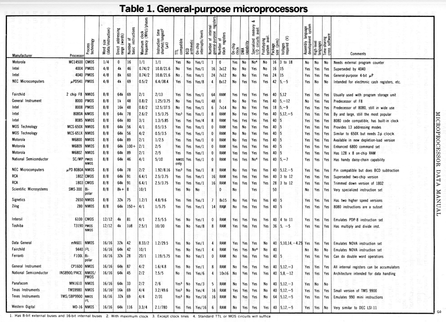
Appendix3 - Comparison Table of Contemporary Microprocessors
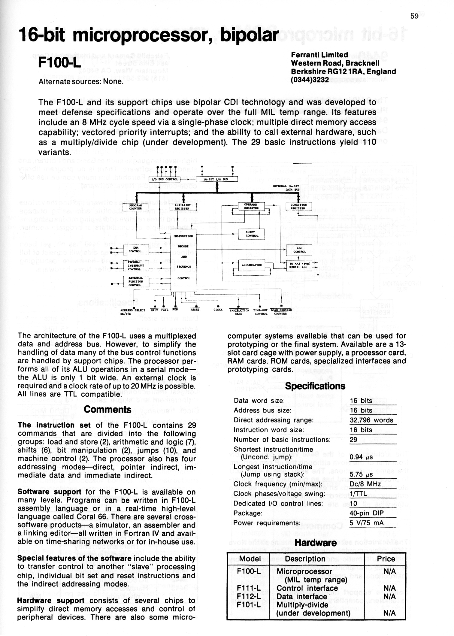
Appendix4 - One Page Ferranti F100L Datasheet
Appendix5 - F100-L Family Silicon Photo Gallery
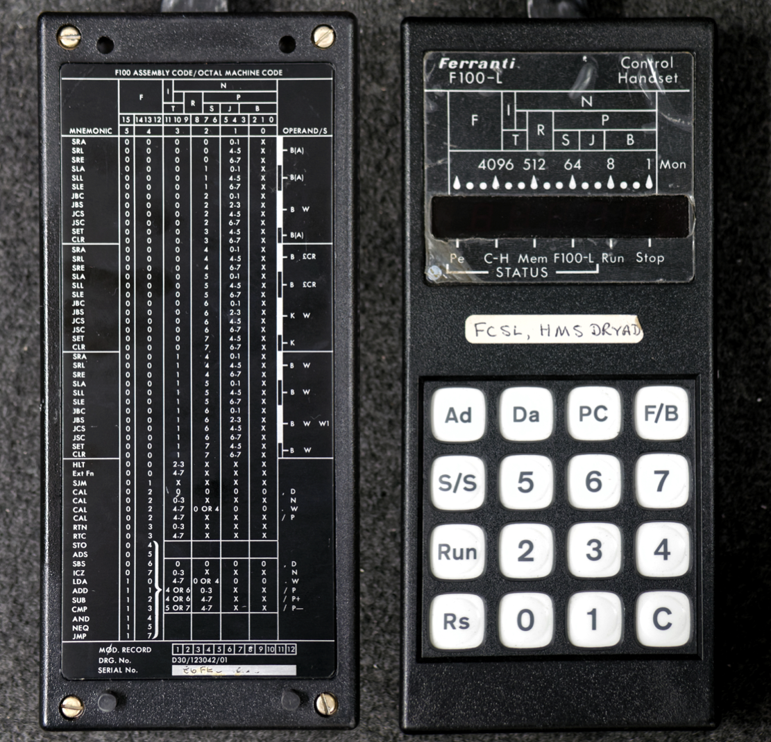
Appendix 1 - The F100-L Microcomputer Control Handset
A handset from the F100-L microcomputer, originally from an installation in HMS Dryad, is held in the collection at the Centre for Computing History, Cambridge, UK: Box704.
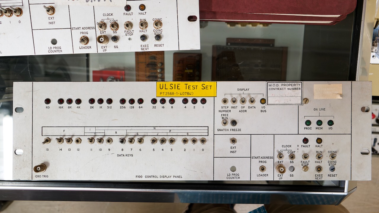
A front panel from a British Military Ptarmigan test installation.
Photographed at _Jim Austin’s Computer Museum in Yorkshire: https://www.computermuseum.org.uk
Appendix 2 - F100-L Handset Assembly Language Summary
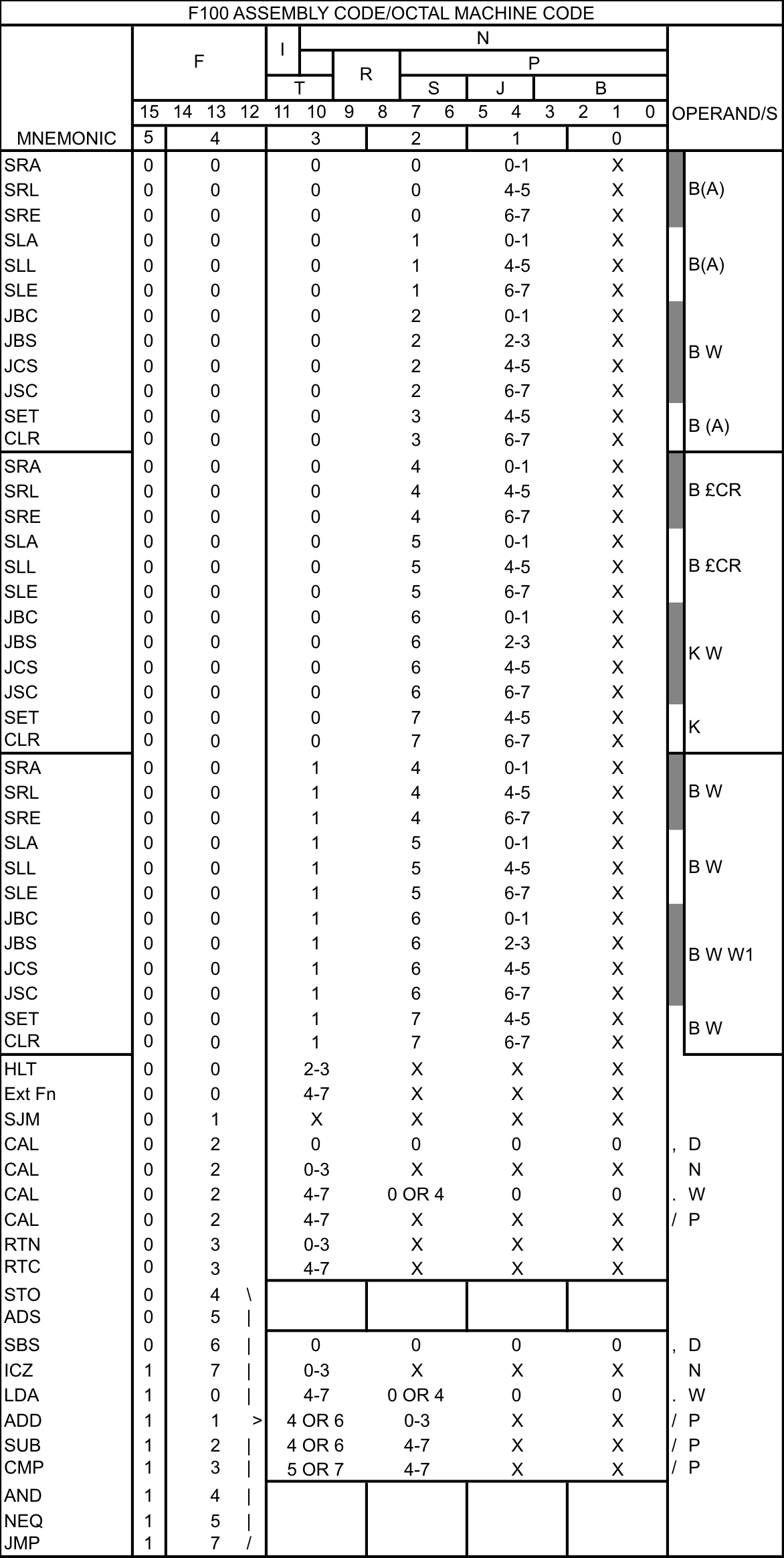
The following table is a transcript from the back of the F100-L microcomputer controller handset
Appendix 3 - Comparison Table of Contemporary Microprocessors
The following table is reproduced from [15]
Appendix 4 - One Page Ferranti F100-L Datasheet
The following datasheet is reproduced from [15]
Appendix 5 - F100-L Family Silicon Photo Gallery
Ferranti F100-L CPU
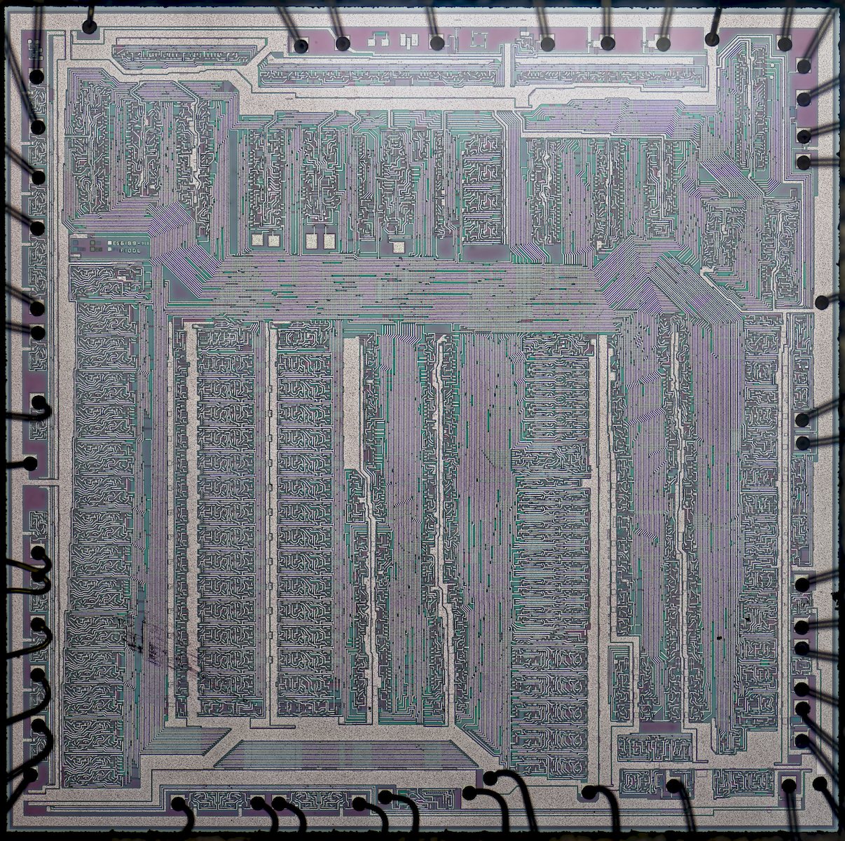
Ferranti F100L AJ BSS2 FRD 8630
Die measures approximately 5.8mm x 5.8mm
F111-L Interface Set Control Chip
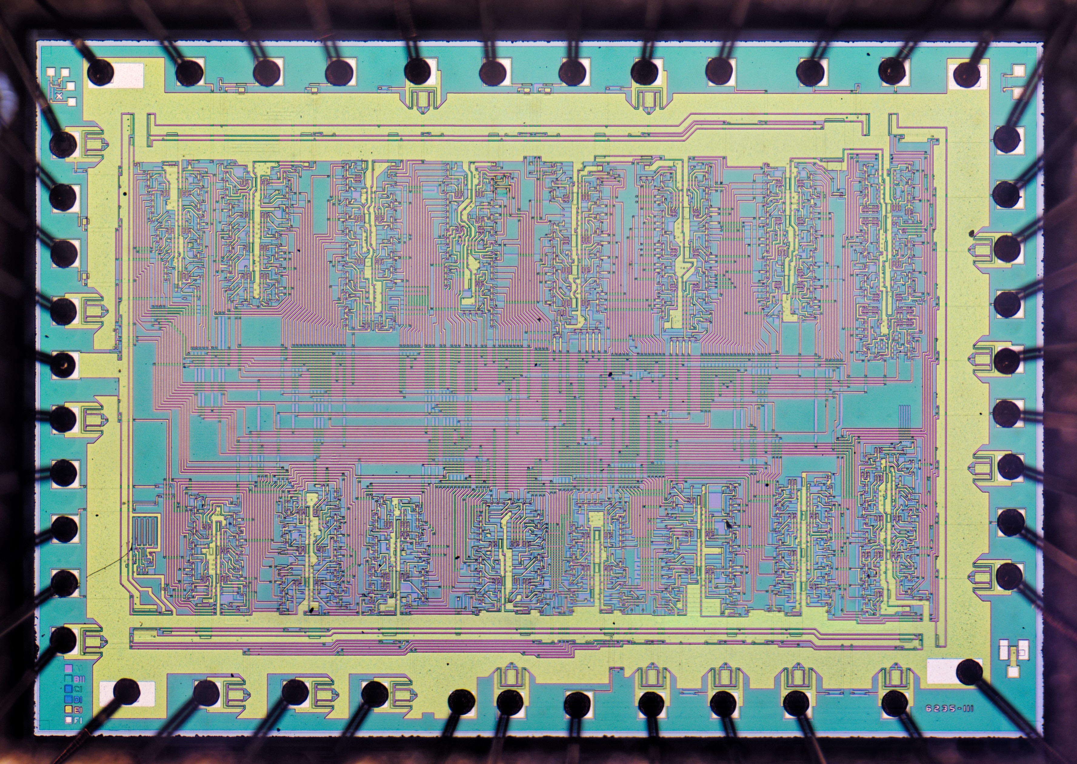
Ferranti F111L AJ BSS2 8103
Additional die marking: 6235-111
Chip Die measures approximately 4.3mm x 2.9mm
F112-L Interface Set Data Chip
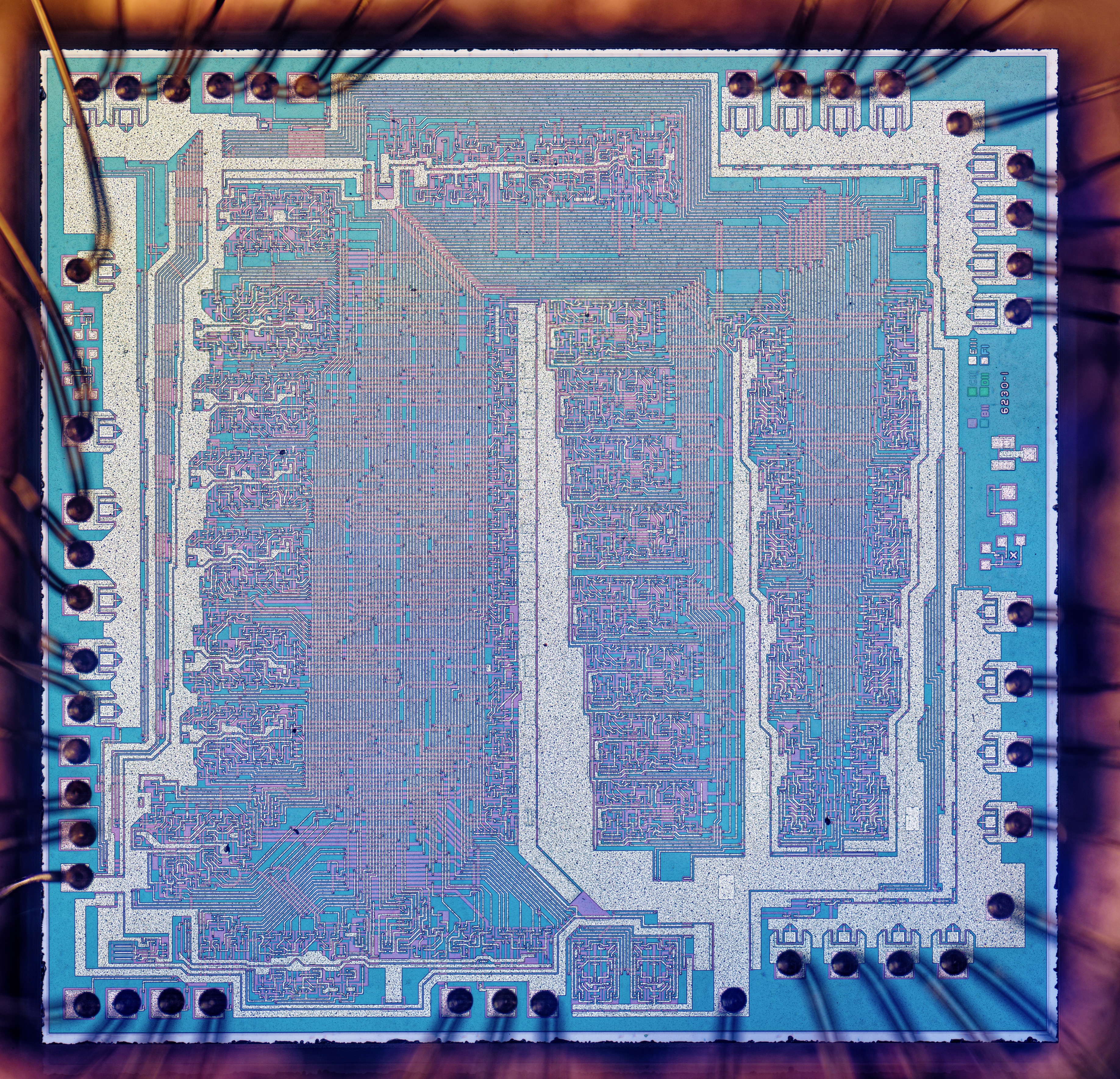
Ferranti F112L AJ BSS2 8515
Additional die marking: 6230-1
Chip Die measures approximately 3.6mm x 3.7mm
F113 High Speed Memory interface chip.
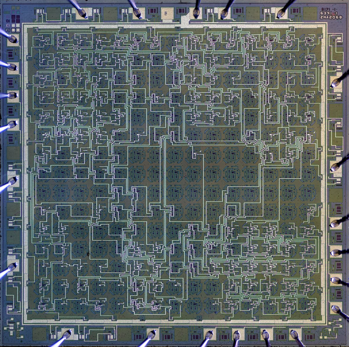
GPS F113LAJ CS 9522A
Implemented on a ZNA2068 ULA, with an array of 15x15 logic elements.
Chip Die measures approximately 3mm x 3mm.
F115 Real Time Interrupt chip.
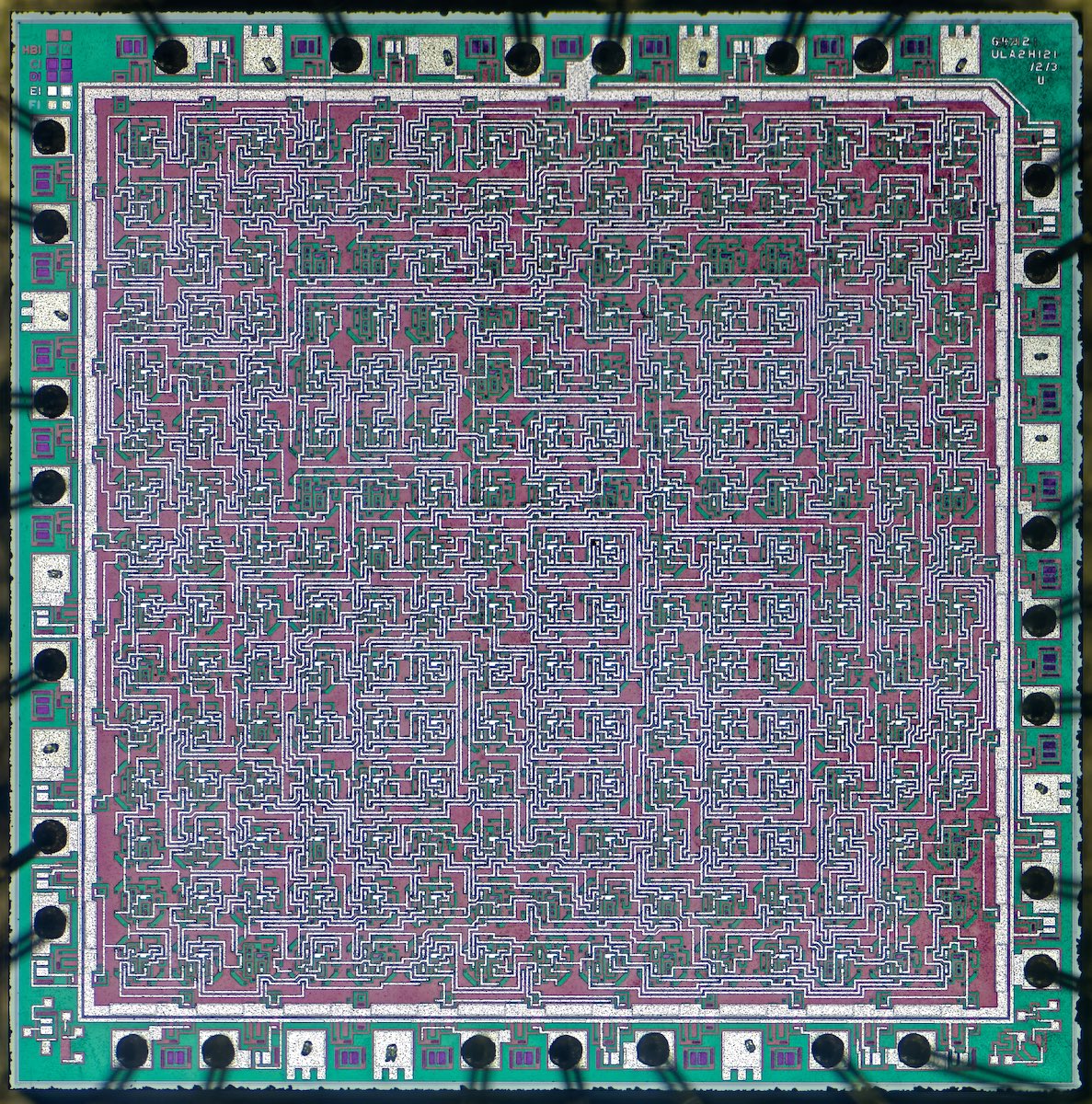
Ferranti F115L AJ BSS2 FRD 8636
Die size: approx 3.3mm x 3.3mm.
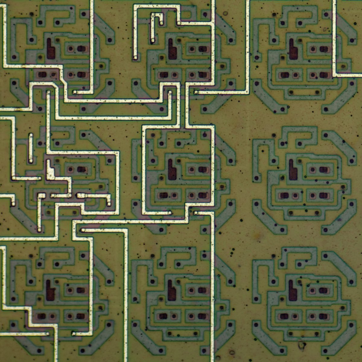
Detail of ULA 2000 series bipolar gate array elements on the F113